Circuit description
|
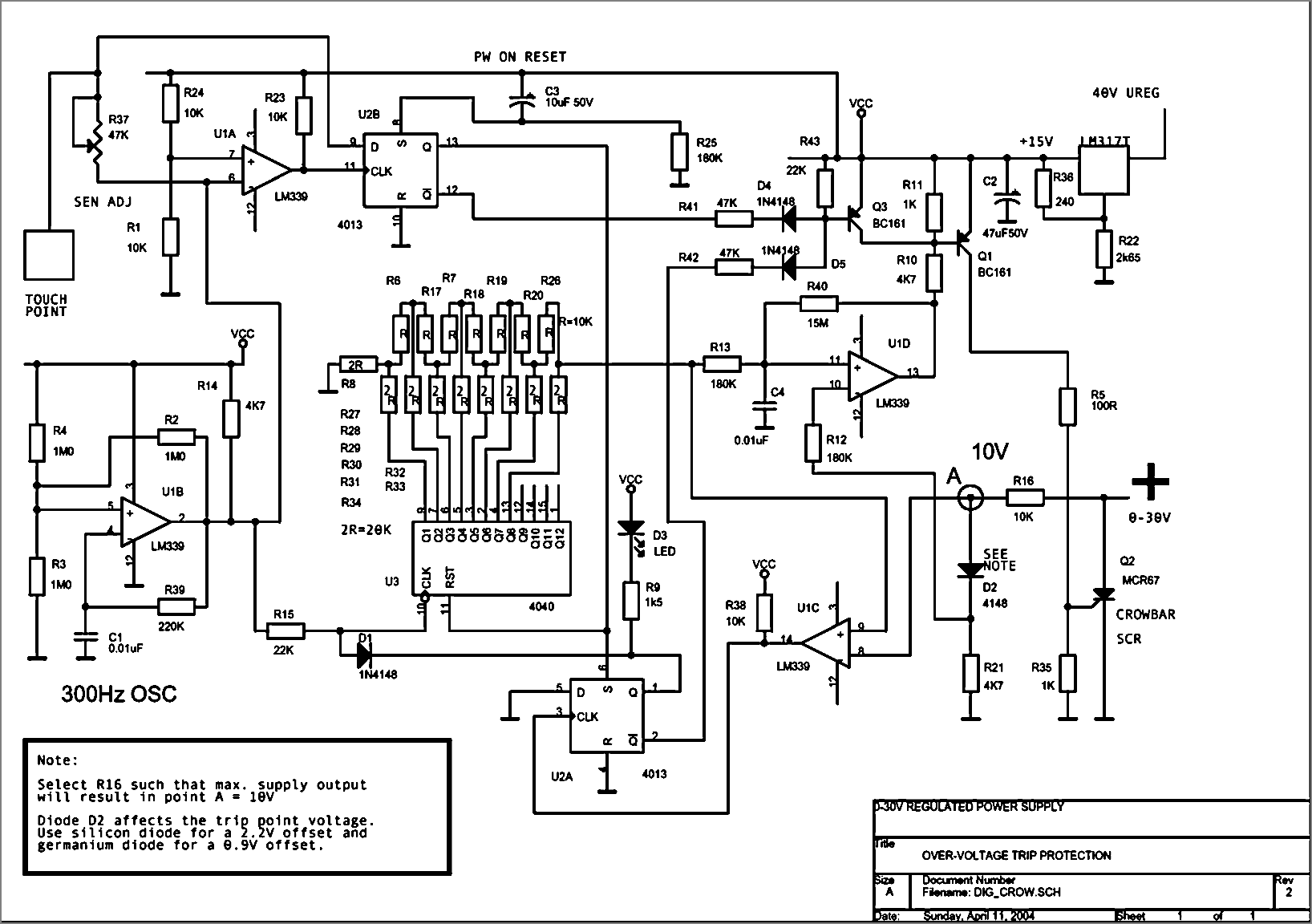
Traditional crowbar circuit on regulated power supply is designed for fixed voltage output only as the trip point must be hardwired. The lack of overvoltage protection on a variable voltage output power supply always make me feel uneasy when I have to connect circuits to be tested or repair to such power supply. The following circuit is developed to provide crowbar protection on a regulated power supply with 0-30V output, using only two CMOS ICs and one voltage comparator IC. The circuit is powered at 15V via a 3-terminal regulator LM317T connected to the main rectifier smoothing capacitor. Common 7815 is not applicable because of its low maximum input voltage. The circuit consists of an oscillator, touch operated switch, digital sample & hold circuit, trip voltage comparator and crowbar SCR. The touch point is made to the metal knob or the metal spindle of the variable resistor that operator adjusts to change the regulated supply output voltage. If the said variable resistor is originally mounted on a conductive panel, the resistor case and spindle must be insulated from the panel for the touch sensor to function properly. The oscillator U1B generates 300Hz squarewave that feed the digital sample & hold circuit and the touch switch. The clock polarity is inversed via U1A before being fed to the U2B 4013 clock input. The 4013 F/F samples the data input 'D' during the rising of the clock. Consider the case where the metal knob is not being touch. Because of the delay cause by U1A, 'D' will always be low while clock rises. When operator changes the power supply output voltage, the metal knob is being touched. The human body would effectively introduce capacitance resulting in delay to signal applies to 'D' and a changed state occurs at the 4013 outputs. While the operator adjusts the supply output voltage, the touch switch operates. U2B changes state and sets U2A. Q3 conducts and trip circuit Q1 is disabled. U3 4040 is forced into reset with all its outputs (Q1-Q8) low and no voltage appears at the R-2R ladder network. Green LED turns off to signal protection circuit is now out of commission. After the correct output voltage is set, operator releases the metal knob and touch switch resets. Diode D4 becomes inactive and reset line of 4040 returns to low. 4040 starts counting up. When the voltage output at the R-2R network matches that of the regulated supply output voltage at point A, U1C operates to enable U2A to change state. This results in bypassing clock pulses from 4040 and turns on the LED. Simultaneously, the trip circuit is armed. However, as the sampling point of the trip comparator U1D pin 10 is taken after diode D2; a voltage offset exists between the R-2R network voltage and the pin 10 voltage. It is this offset voltage that gives the ceiling of the overvoltage protection. As the input is sampled via R16 & R21 voltage divider, this translates to 300% of the diode voltage drop added to the external voltage that would result in a trip. Choice of D2 between germanium or silicon types gives different trip ceiling voltage. The test results of the actual tripping voltage on my prototype were measured as follow:
|