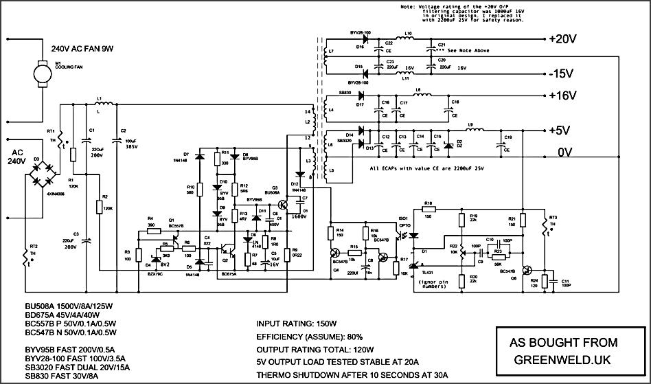
Circuit description
|
Note: The component designation in schematic diagram is automatically assigned by the Schematic Capture program and is not amended to follow the actual circuit board photo. All reference to component is based on the schematic diagram. You will need to download the PDF and print the circuit out in order to read the components clearly and to follow the discussion of the rest of this webpage.
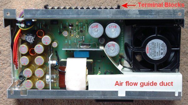
GENERALThis is an old new stock 150W switching supply(item #Q6103) sold by GreenWeld for £4.99. The date of manufacture dated back to 1984. It operates off AC240V supply and provides the following voltage outputs: +5V, +16V, +20V and -15V. The whole case is made from 2mm folded aluminum sheet in two parts and can be easily separated. The AC connection is via IEC socket and the unit come fitted with a 75mm AC240V cooling fan. The noise of the fan is horible but the cooling effect is wonderful. Do not attempt to use this for your PC as the 16V output is too high and will damage the PC component. |
 |
INPUT SECTIONAC240V is rectified by the four bridge-connected 1N4006 rectifiers and smoothed by two 220uF 200V electrolytic capacitors
connected in series. It then passes through via a choke into the third smoothing capacitor which is 100uF 385V. The in-rush
current is limited via the two thermistors RT1 & RT2. HV SECTIONThe 340V HV then passed through the main switching coil L2(terminals 12 & 14) and transistor Q3(BU508A), then via emitter resistor R9(0R22) to the 0V of the high voltage side. The voltage developed across the resistor R9 represent the instantaneous magnitude of the transistor current. When first powered up, transistor Q3(BU508A) is not conducting and the initial "startup kick" is provided via the two 120K resistors R1 & R2, through winding L3 and diode D8 & R12. Once the transistor is conducting, voltage is induced in the winding L3 and the circuit feeds itself. Transistor Q2 performs an important function. When it conducts, it shunt away the base drive to Q3 so that Q3 turns off. It has to do this at the correct moment after Q3 turned on. The precise moment is controlled via feedback signal from the secondary circuit via an opto-coupler. Winding L3, diodes D8,D10,D9,R8 and C5 formed a rectifying circuit with voltage of about 10 volts. Because the positive output of this rectifying circuit D9 is connected to the emitter of Q3, the 10 volt voltage appears between Q3 emitter and winding terminal 8. Or, voltage at terminal 8 is -10V when emitter Q3 is used as an reference point. Conduction of Q2 will thus pulls Q3 base negative and turns off Q3. The conduction of Q2 is in-turn depends on the feedback signal from the opto-isolator. PROTECTION SECTIONTransistor Q1 R3,R4 & R5, Zener D4 formed an overcurrent protection circuit. When Q3 collector current increases, voltage
across emitter resistor R9 also increases. This increase of voltage also built up across R4 390ohm. When this voltage across R4
reaches 0.6V, Q1 conducts and turns on Q2, shutting off Q3. CONTROL SECTIONSecondary circuit TL431C develops a fixed voltage of 3.82V (when O/P=5.00V) regardless of the 5V output voltage when the 5V output is higher than 3.85V. Any increase of the 5V output voltage will result in increase voltage across the photodiode and more light output to the photo-transistor. When one first look at the control circuit, it seems obvious that Q5 and Q4 actively control the output voltage. However, the circuit arrangement means that when output voltage increases, more light will shine on the photo-transistor which makes it conduct more, and Q5 will conduct more leading to Q4 conduct less. This will result in the increase of secondary voltage, which is the direct opposite of reducing the output voltage as Q2 now takes longer to turn on. Faced with this puzzle, the voltages across the components were measured while the unit is on load. The voltage across the capacitor C8 was found to be 0.18-0.2V. Thus Q4 can not be ON and is always OFF. Then it becomes clear that Q5 and Q4 does not form part of the voltage control circuit but function as a backup protection circuit instead. In normal operation, current flows through photo-transistor and R17(10K) to base of Q2. This is a small current so now it also becomes apparent why a Darlington transistor Q2 is being used. The voltage across R17 also turns on Q5, shunting the capacitor C8. Without base drive Q4 is always OFF. However, if the sensing path failed for whatever reason, Q5 turns OFF and C8 charges up. Q4 conducts and turns ON Q2. When the secondary output voltage increases, the increase in photo-transistor current resulted in Q2 is turn on earlier and shunt
off the Q3 base drive earlier. As a result, less current is flowing in the main switching coil and the secondary voltage then decreases.
Thus a negative feedback path resulted and output voltage is stabilised. RECTIFY SECTIONThe rectifying circuit is fairly standard and easily understood. Besides labelling as 150W on the casing, there is no other indication of the voltage or current rating of individual output of the switching supply. The rating of the 5V output is loaded to 25A and then increased to 30A. The unit then regards this as overload and shutdown after a while. Please note that the common of the 16V output is sitting on the +5V rail and so without main current flowing in the 5V winding, only small current can flow in the 16V output.All the other voltages beside +5V is not meant for heavy loading but serve as some sort of control purposes. I would recommend less than 1A be drawn from any of these output, even with suitable loading on the +5V output. When there is no loading on any of the outputs, the switching supply enters an keep alive pulse mode of period of 0.3 seconds. This is clearly audiable as "click" sound from the transformer core. At no load, one output measured +20V but the capacitor C21 used originally was 1000uF 16V. The output could well be falling to 16V under load but for safety reason capacitor C21 is replaced by one with 25V rating. I haven't got one for 1000uF so I put in
a 2200uF 25V capacitor instead. MODIFICATIONThe original AC cooling fan is mounted in a such a way that the whole power supply must be used in a vertical position. This is very inconvience and thus the fan was relocated to the other side of the case. The original fan opening was blanked off. This modification allow the unit be lay flat on the bench with the supply inlet at one side. To prevent the air flow from short-circuiting it self, an air flow guide duct was made using stiff insulation material. Terminal block is added to the side of the case to ease the connection of different voltages. The cooling fins of the Q3 and Q2 were not of adequate size and require
forced air circulation. Both aluminium cooling fins are "LIVE" . It might be possible, under light load, to do away with the nosiy fan by using the aluminium casing as a heatsink. This would involve putting in extra electrical insulated aluminium plate/block for Q3 & Q2 and bolt these
plate/block to the casing. Alternatively, an 12V DC fan can be used instead which is much simplier. Anyway, the heatsinking of
Q2 should be improved to enhance good reliability when total air flow is reduced. |