Microchip PIC 16F628A Microcontroller
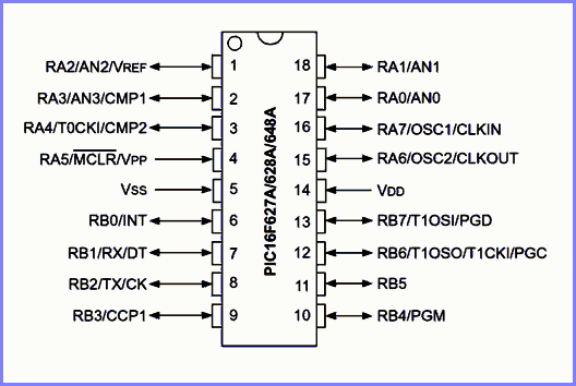
To make a start, let us take a look at the most popular member in the medium range PIC. The diagrams in the follow tutorials are all extracted from the datasheet of 16F628A. Microchip has done a very good job of making the detailed datasheet and it includes nearly everything one needed to get started. The complete 35 instruction set are also included too. The plastic Dual-in-line package with 0.1 inch pin spacing is used most by hobbyist and its pinout is shown below. You can download the 16F628A datasheet here if you have not already done so:Microchip Datasheet download Link
Microchip PIC 16F628A Microcontroller
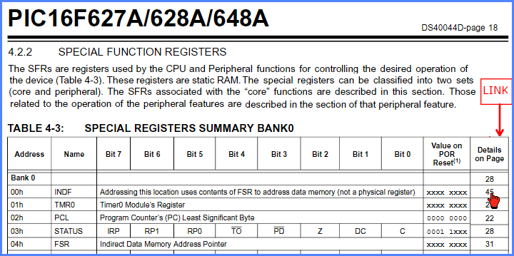
You will notice that there are usually more than one names labelled to each pin, except the two power supply pins and pin11 in this case. This indicates that a particular pin can serve different functions. The user can select the intended function by setting/clearing bits inside certain registers in the internal of the PIC. These are called special function registers(SFR) and they are 8-bit wide. You can read about the SFR on page 18 of the datasheet. Notices that at the end of each item shown in the datasheet pdf file, the page number is actually a link to goto the page that describe fully about the said register. All SFRs has unique name in capital letters which one should use to make reference to them in writing program codes.
I/O is a short form for input/output and port means location(s).
The term "R" in the pinout diagram is used to denote ports. RA is port A and RA2 is bit2 of port A. Similarily, RB, RC, RD and RE refers to port B to E in general, if they are available. RX, however, is not port X but the receive pin for UART and so as the TX pin.
Notices also that there are arrow associates with each pin and this indicates that the pin can be used as input, output or both. Note that the PIC reset pin MCLR pin4 is strictly an input pin only because of hardware and programming requirement. This prevents one from using port A as a 8-bit output port. Pin10 RB4 also needs particular mentioning. The name of this pin is PGM which decides the programming method where external user object code is being programmed(shifted) into a PIC. If one uses the low voltage programming method(LVP), then this PGM pin must be connected to logic LOW during PIC normal operation. Thus one would lose the ability to use this pin as digital I/O, which in effect, means losing the ability of using Port B as a 8-bit I/O port. The solution/alternative is always use only the high voltage programming mode(HVP) discussed later.
If a certain pin is setup up by user as an input, then the pin will have a high input impedance of over a few megaohms(Mohm)and in general will not cause any loading to the signal source. So a logic signal or voltage between 0-Vdd supply voltage can be safely applied without problem. As with all CMOS integrated circuit design, there are protection diodes connected from the pin to both supply rails so that the PIC is well protected from static discharge. These diodes are not and should not be conducting in normal use. The only chance that they would be conducting is when a voltage higher than the supply voltage or a negative voltage is applied. Large current will then flow and this will destroy the PIC. To prevent this from happening, a large series resistor is required to limit the resultant diode current should there are any possibilities that the input voltage can go out of range. Usually, an input current of one milliamp(mA) or less would be considered safe for a pin.
When a pin is configured as output, it can source or sink a maximum of 25mA each but when more than one pin is driven, the allowable total maximum current for port A & B together is limited to 200mA.
Years ago, in order to program the user code into a PIC, a high voltage of +13V or higher is needed. It is known as the HVP which means high voltage programming mode. This place limitation on the field modification of the user codes on a PIC as +13V might not be freely available. Microchip thus come up with another additional programming option as LVP meaning low voltage programming mode, using only +5V. We were told that the high voltage is then being generated internally within the PIC. Now we have two programming modes and this must then be a bit somewhere that tells the PIC which programming mode it should be configured. To prevent the PIC from entering LVP with normal +5V power supply, a pin is assign to allow user to select/disable the LVP programming mode. This is the PGM pin. A high level would select LVP while a LOW would disable it. The bad news is that this arrangement taken oven one of the bits in RB and one cannot use portB as a 8-bit port. The solution is simple, never enable LVP therefore the PGM pin is then available as normal I/O pin.
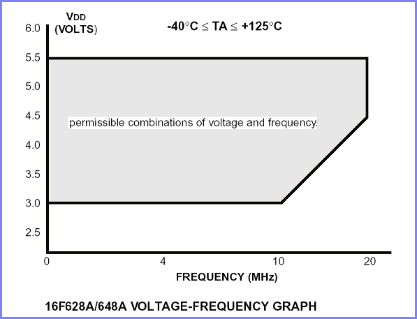
The family of PIC is based on CMOS design so some of them(but not all, check datasheet)can work on a voltage range of 5.5V to 3V, with the nominal being 5.0V. The 16F628A is such a PIC. However, with reduced supply voltage, the maximum crystal or clock frequency is also retricted to lower values. The supply current drawn for 16F628A alone is only a few milliamps(mA) so it is usually possible to power the PIC directly using a pack of batteries. A particular series of LF PICs would allow even lower supply voltage down to 2.0V but usually with reduced crystal frequency. The following graph shows the range of voltage and crystal frequency that applies to 16F628A.
Normally a microcontroller chip uses two pins for the connection of a crystal as the clock frequency. However, on a 16F628A there are eight ways to make changes to this. For a start, the two pins can be configured to act as low-power crystal(32KHz-200KHz)osc, crystal/resonator(100KHz-4MHz) and high-speed crystal(8MHz-20MHz) osc. What will be the correct mode to choose should the user uses a crystal of 6MHz is not mentioned in the datasheet so both mode can be used. As a rule, idle current consumption would increase from one mode to the next.
In the next three modes, one of the two pins can be configured as an input for external clock pulses, or acts as input for an external RC oscillator, while the remaining pin provides the clock pulses output to drive other circuit. Or the user can configure the remaining pin as digital I/O. One very interesting feature of external RC oscillator is the ability to change clock speed under software control. Using an digital output pin and a suitable resistor, the clock speed of the PIC can be changed by setting a HIGH to the output pin or reprogrammed the pin as an input.
The last two modes concerns using internal oscillator and freeing up both clock pins. The remaining pins can be set to clock pulses output or simply as a digital I/O.